|
|

|
|
| Partname: | AD7394AR |
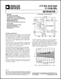
| Description: | 0.3-7V; 50mA; dual, serial input 12/10-bit DAC. For automotive output span voltage, portable communications, digitally controlled calibration, PC peripherals |
| Manufacturer: | Analog Devices |
| Package: | SOIC |
| Pins: | 14 |
| Oper. temp.: | -40 to 85 |
| Datasheet: | PDF (268K).
Click here to download *) |
The full-scale output voltage is determined by the applied external reference input voltage, VREF. The rail-to-rail VREF input to VOUT outputs allows for a full-scale voltage set equal to the positive supply VDD or any value in between. A doubled-buffered serial data interface offers high speed, microcontroller compatible inputs using serial-data-in (SDI), clock (CLK) and load strobe (LDA + LDB) pins. A chip-select (CS) pin simplifies connection of multiple DAC packages by enabling the clock input when active low. Additionally, an RS input sets the output to zero scale or to 1/2 scale based on the logic level applied to the MSB pin. The power shutdown pin, SHDN, reduces power dissipation to nanoamp current levels. All digital inputs contain Schmitt-triggered logic levels to minimize power dissipation and prevent false triggering on the clock input. |
|

Click here to download AD7394AR Datasheet*) |
 |
| *)Datasheets downloading from ChipDocs is only for our members (paid service). REGISTER NOW for your membership. |
|
|
|

